
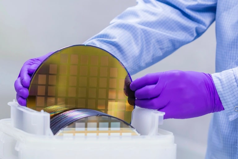
Have you ever wondered how your phone, computer, or tablet actually works inside? The secret lies in something smaller than a coin, yet powerful enough to run modern technology. It all starts with wafer fabrication.
This process builds the tiny parts that power electronic devices. Even though it happens behind the scenes, it’s one of the most important steps in making electronics.
By the end of this post, you’ll clearly understand how wafer fabrication works and how it helps create the devices you use every day.
What Really Happens in Wafer Fabrication?
Wafer fabrication is the process of making the base of a microchip. Microchips are like the brains of electronic devices.
The process takes place in high-tech labs called clean rooms. These rooms are super clean because even a tiny speck of dust can ruin a chip.
The main goal of wafer fabrication is to build tiny circuits on thin, round pieces of material. These are called wafers.
Each step in this process must be perfect to make sure the microchip works well. It takes many steps to build one chip, and most of the work is done by machines with extreme accuracy.
Starting with Pure Silicon
The process begins with a material called silicon. Silicon is found in sand and rocks, and it’s great for conducting electricity.
But to be used in electronics, it must be purified. This means all other materials are removed so that only pure silicon remains.
The pure silicon is melted and turned into a long crystal, called an ingot. This ingot is then sliced into very thin discs.
These discs are called silicon wafers. They are flat, smooth, and ready to be turned into tiny circuits. These wafers are polished so they have no scratches, which is important for building the layers of the chip.
Patterns That Shape the Chip
The next step is to create patterns on the wafer. These patterns tell the chip what to do. This step is called lithography. In this step, a light-sensitive material is added to the wafer.
Then, light is used to draw tiny shapes on it. These shapes are smaller than a piece of dust, yet they form the paths that carry electricity inside your device.
Lithography is like shining light through a stencil to make an image. The wafer is coated with a thin layer of photoresist. Light passes through a mask to mark the pattern.
Where the light hits, the photoresist changes. The unwanted parts are then removed, and the pattern remains on the wafer.
Carving the Patterns with Etching
After the pattern is made, it must be carved into the wafer. This is done with a process called etching.
There are two types of etching: dry and wet. Dry etching uses gases, while wet etching uses liquids.
Etching removes the parts of the wafer not protected by the photoresist. This step makes the patterns real by cutting them into the surface.
Etching must be done carefully, as mistakes can damage the wafer. Once the etching is done, the photoresist is cleaned off.
Changing the Material with Doping
Now the wafer is ready for doping. This means adding small amounts of other materials to the silicon.
These materials change how electricity flows through the wafer. Some areas are made to carry more electricity, while others are made to block it.
Doping is done by putting the wafer in a chamber filled with gas. The gas contains the new material.
Heat or electricity is then used to push the atoms of the gas into the wafer. This creates special areas that help the chip do its job.
Adding Layers and Building Up
The chip is made of many layers; each layer is added one at a time. After each new layer, lithography, etching, and doping are repeated. This adds more parts to the chip, like wires, switches, and connections.
Building a chip is like making a sandwich, but with many thin layers stacked on top of each other. Each layer must line up perfectly with the others.
Even the smallest mistake can ruin the chip. This is why the process takes so long and needs special machines.
Making Sure It All Works
After all the layers are built, the wafer is tested. This is to make sure everything works as planned. Tiny needles touch each chip on the wafer and check for power, speed, and proper connections.
If a chip does not pass the test, it is marked and removed later. The good chips move on to the next step, where they are cut from the wafer and packaged. Each chip is placed inside a case that protects it and allows it to be used in electronics.
From Factory to Everyday Life
Once the chips are packaged, they are sent to companies that build computers, phones, and other devices. The chip is placed inside the device, where it controls how the device works.
Even though you never see it, wafer fabrication plays a huge role in your daily life. Without it, there would be no smartphones, video games, or smartwatches. Every button you press and every screen you swipe works because of this tiny chip.
Why This Process Matters to Everyone?
Wafer fabrication may sound like something only scientists care about. But it affects everyone.
The better we get at making chips, the faster and smaller our devices become. It also helps companies create new technology like self-driving cars, smart homes, and health trackers.
This process is also important for saving energy. Modern chips are built to use less power while doing more work. That means longer battery life for your devices and less impact on the planet.
Understanding how wafer fabrication works helps us see the value in the tech we use. It also helps young learners think about careers in science and engineering. If you like solving problems and using tools, you might enjoy working in this exciting field someday.
The Incredible Process Behind Your Everyday Tech
Now you know what makes your favorite electronics work. Wafer fabrication is a careful process that brings together science, machines, and tiny patterns. From pure silicon to high-speed chips, every step matters.
Thanks to wafer fabrication, we enjoy smart devices that keep us connected, help us learn, and make life easier. This guide showed you the main steps, like lithography, etching, and doping, that power modern electronics. Next time you use your phone or tablet, remember the hard work behind that little chip.
Did this guide help you? Browse the rest of this section for more advice on a variety of topics.
